USB3 video bridge
Until now, differences in their frame formats and signaling mechanisms made it difficult for HD video cameras, image sensors and other AV sources to exchange their uncompressed HD audio/video content across a USB3 connection.
Finding a simpler way to move HD video across a USB connection has become increasingly important as PCs become an integral part of a growing number of industrial, commercial and consumer applications. This includes machine vision systems (USB3 video and vision cameras), video production products (video converters, video capture devices), digital signage, surveillance, and even mobile consumer gadgets.
This article will introduce an encapsulation technique which provides a transparent pipeline for nearly any multimedia stream within a USB channel, and how it can be implemented using a new breed of small, inexpensive, low-power FPGAs.
We’ll be referencing the USB3 video bridge reference design as a practical example which addresses the needs of many PC-based applications in consumer, video broadcast, machine vision, and surveillance systems.
Although USB3 technology finally gives PCs the I/O bandwidth they need to support uncompressed HD video/audio streams, it’s had difficulty realizing its full potential in media processing applications because most USB connections aren’t available on most commonly-used video and multimedia equipment.
For example, HDMI interfaces are a de facto standard for consumer video products, most professional video equipment relies on SDI ports and the image sensors used in industrial and scientific applications frequently use either sub-LVDS or MIPI CSI-2 interfaces. While it’s relatively easy to convert the different electrical signals used by the PHY layer of each interface into data streams which can be processed by standard digital logic, their frame structures and signaling protocols are radically different.
Traditionally, the best solution to this “digital disconnect” between the PC’s USB ports and AV equipment’s SDI/HDMI connections was to work around it.
This usually involved a frame grabber card which could capture the video data, encapsulate it within PCI Express data packets and move it directly onto the host system’s data bus. Although it works well, a frame grabber also adds enough cost and complexity to a design that it’s unsuitable for many applications.
The digital disconnect can also be spanned with a packet bridge which performs real-time format conversions between an AV device’s output and the host system’s USB3 interface.
These bridges provide a simpler, more flexible, cost-effective alternative to frame grabbers by employing one or more of the bridging mechanisms defined in the USB standard for encapsulating multimedia streams within USB packets and reassembling outgoing streams back into their native format.
Webcams and other USB media devices already have these encapsulation mechanisms built into their electronics but there are few, if any, off-the-shelf ICs available capable of bridging HD video at USB3 speed.
The USB standard already includes well-defined bridging protocols for HDMI, SDI, and almost every other commonly-used digital media interface. The most commonly-used of these is the USB Video Class (UVC) which defines the characteristics of USB-connected video devices like webcams, digital camcorders, transcoders and analog video converters.
UVC supports most common frame- and stream-based video formats, including frame-based standards such as MJPEG and DV used by most of the applications described in this article.
These high-quality/high-bandwidth formats typically transmit their frames as uncompressed YUV (YUY2, NV12) data with a separate out-of-band channel for the frame/sample boundary information. While not directly applicable to this application, it should be noted that UVC also supports compressed stream-based video formats, including MPEG-2 TS, MPEG-2 PS and MPEG-1 as well as temporally encoded video formats like H.264 and VP8.
In PC-based applications, UVC provides a method for encapsulating video data and control signals from a camera or other source, within standard USB packets for transport over the USB3 link to the host PC.
The host PC then replays the received video data using a standard Microsoft UVC driver and a compatible application. Stand-alone audio streams (not associated with a video stream) are accommodated in a similar way using the USB Audio Class (UAC) 2 format
Ideally, a USB video bridge should be able to convert streams from several video interfaces (HDMI, Tri-rate SDI, CMOS Sensor serial and MIPI CSI-2 etc…) and sensor outputs into standard UVC packets and transfer the data packets over the USB3 link to the host PC. In addition to supporting video streams, the bridge should also act as an interworking conduit for multi-channel I2S UAC-compliant audio content.
To accomplish these tasks, the bridge must perform two important functions:
1) Electrical Conversion – The electrical signals from the incoming media source must be recovered, synchronized and converted to a serial bit stream which can be processed and encapsulated within USB packets. The bridge must be able to accept inputs from HDMI, MIPI, and SDI A/V interfaces and support a USB3 MAC/PHY host system connection.
Some FPGAs include analog circuitry required to support the PHY layer transmit/receive functions of one or two commonly-used interfaces, they can also be implemented with the addition of readily-available commercial devices. The next section will provide details on how this is done.
2) Format conversion – The data and control streams associated with the HDMI, MIPI, and SDI interfaces must be encapsulated within the in UVC format and transmitted to the host system via a USB3 bus transceiver. In addition it must provide buffering between its video input sources, which are received in high-speed bursts, and the relatively steady transfer rate of the USB3 interface.
To conserve bandwidth, the video’s blanking interval is dropped before conversion so only active video data are transmitted in UVC packets. Audio data not associated with a video stream is transferred via USB’s isochronous mode.
The bridge must also be able to process the outputs of commonly-used image sensors into a format which can be processed by the USB interface. This includes serial outputs such as the MIPI CSI-2 used in most mobile applications and the subLVDS format used by Panasonic and Sony image sensors.
It also needs to accept the parallel outputs of digital signal processors (DSPs)3 and other devices used to control and process the outputs of advanced image sensors used in scientific and industrial applications.
In order to deliver the necessary performance, configurability, solution cost and time-to-market, this multi-interface bridge uses an FPGA to implement as much of its functionality as possible, with only a handful of external components to support the MAC/PHY portions of the interfaces.
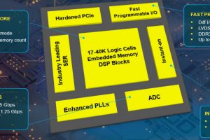
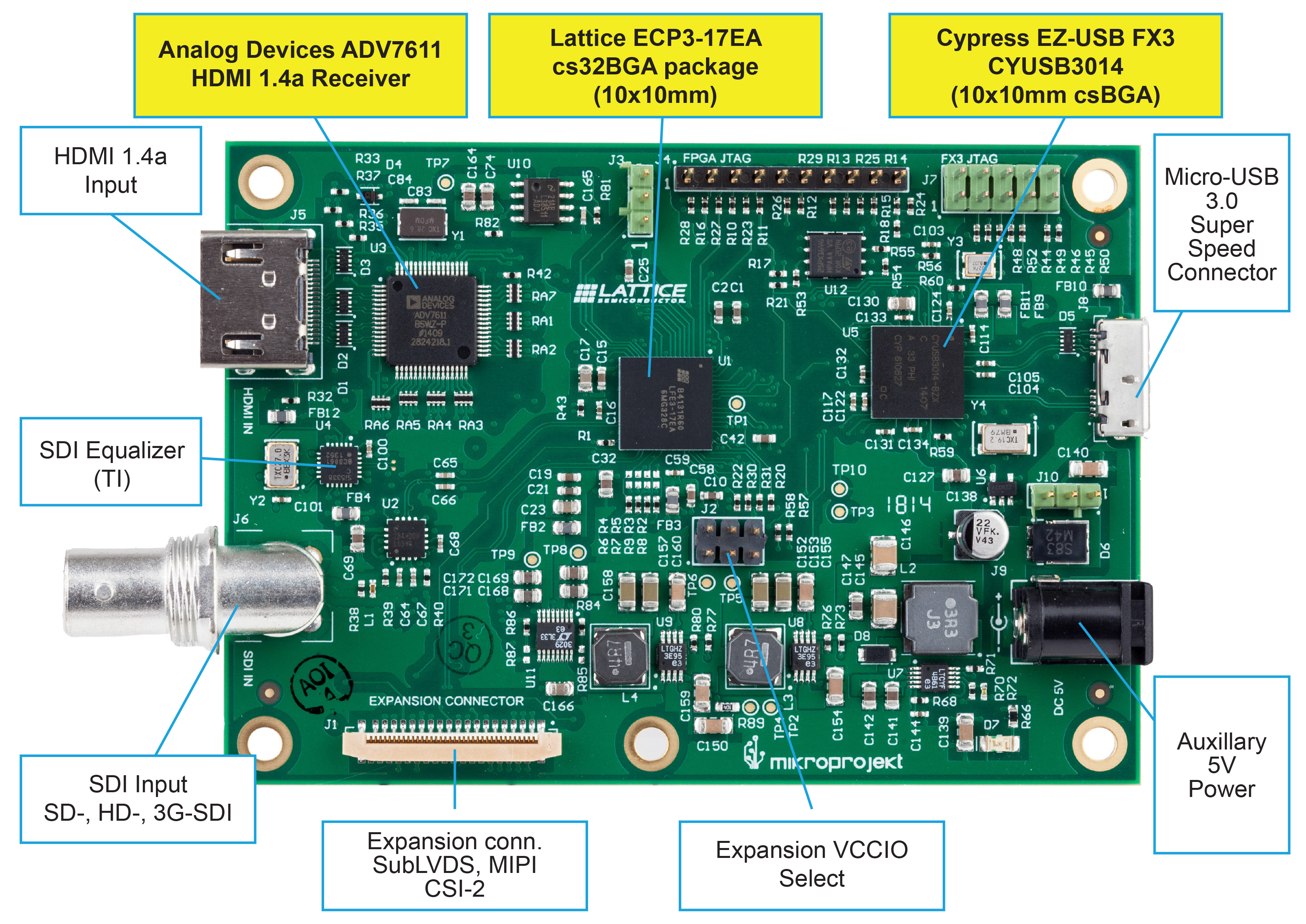
A member of Lattice’s ECP3 FPGA4 family (LFE3-17EA), was selected for this design because it has the necessary FPGA resources required, such as high-performance I/O, speed and size and contains several hardware cores which implement key functions used in this application. These pre-integrated building blocks, such as multi-lane SERDES transceiver and SDI PHY , simplies the design and further reduces its total solution cost.
The resulting solution supports high speed reception and packing of video and audio data into USB 3.0 UVC and UAC data frames without the use of external memory buffers.
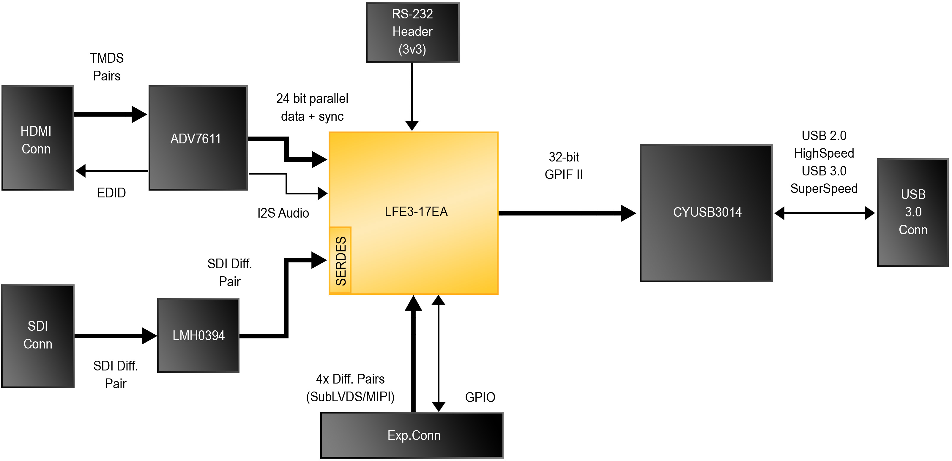
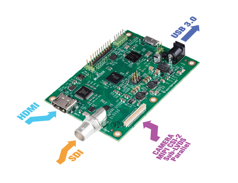
Component-level block diagram of the FPGA-based USB3 bridge
As shown in the block diagram below (Fig.2), each of the PHY-specific transceivers surrounding the FPGA provide timing, handshake and voltage level translation between the media stream signals and the FPGA’s logic level I/O pins.
Fig.2: Component-level block diagram of the FPGA-based USB3 bridge.
All sources and outputs in this design use a similar parallel bus structure (Parallel Data + HS + VS +DE) to interface to the processing elements created within the FPGA. We’ll discuss why this is important after we review each of the PHY interfaces supported by the video bridge:
A TI LMH0394 equalizer adjusts the incoming signals before feeding them to the FPGA’s on-chip Tri-Rate SDI PHY hardware core which supports all three SDI data rates (SD, HD and 3G).
HDMI data is received via an Analog Devices ADV7611 which supports the HDMI 1.4a standard for professional audio and video signals and includes an optional HDCP decoder. If the video source in your application is not HDCP encrypted, additional savings can be realized by implementing an HDMI receiver within the FPGA and eliminating the hardware receiver.
An expansion connector allows the connection of a camera or sensor over either the MIPI CSI-2 interface, or SubLVDS differential lines, quickly transforming the bridge into a USB 3.0 High Definition camera suitable for industrial vision applications.
An image sensor’s video data is received through one or more of the expansion connector’s four serial data lanes and converted to the common parallel interface. The FPGA-based functional blocks which support the CMOS sensor (subLVDS) and MIPI CSI-2 serial interfaces also includes CMOS sensor image processing functions such as deBayer, and/or color space conversion and scalar processing.
Once video and audio data is encapsulated within USB packets, it’s sent to a Cypress CYUSB3014 SuperSpeed USB Controller, a 5-Gbps PIPE USB 3.0-compliant PHY which serves as the bridge’s connection to a USB host system ( 5Gbit/s ). The USB PHY interfaces to the FPGA via its on-chip 100-MHz GPIF II parallel interface (configured for a 32-bit bus width).
The FX3 also contains an embedded 200MHz, 32-bit ARM9 RSIC core, equipped with I2C and SPI interfaces. This allows it to perform the setup and configuration of all chips on board, including initialization of the ADV7611 and LMH0394.
It is also able to configure the FPGA via its Slave SPI interface, and perform design control functions its via I2C connection. The ARM’s software and the FPGA’s bitfile are stored in the SPI flash connected to Cypress USB3 Controller chip External JTAG connector allows direct design download and reveal debugging in the FPGA.
Most of the programmable IP cores created within the ECP3 FPGA are concerned with recovering, buffering and encapsulating the incoming video data within the UVC format and transmitting it to the CYUSB3014 USB bus transceiver. The FPGA is also used to implement several other critical functions, shown in the functional block diagram below (Fig.3).
Fig.3: Most functional elements of the USB video bridge can be implemented on a Lattice ECP3 FPGA. (Courtesy of Lattice Semiconductor)
As mentioned earlier, the USB PHY and each of the video sources in this design use a similar parallel bus structure (Parallel Data + HS + VS +DE) to interface to the processing elements created within the FPGA. While each device may have a different bus width, the common architecture allows them to construct powerful FPGA-based processing elements which can packetize and transform nearly any video/audio format in an efficient manner.
For example, the data bus between FPGA and Cypress FX3 (a.k.a GPIF II interface) is 32-bit wide while the UVC video format is YUV 16-bit, the I²S audio could be 16-bit or 24-bit. The FPGA’s processing elements can make efficient use of the 32-bit common bus by combining a 24-bit audio sample with the first 8-bits from next sample without burdening the FX3, or “borrowing” any processing cycles from its microcontroller.
Although designed primarily to serve as a training and development tool for Lattice’s customers, the reference design platform has also provided the FPGA manufacturer with many important lessons.
FPGA-based USB video bridge reference design
For example, it helped identify several design issues which affect efficient transfer of slow, isochronous audio data along with the fast and burst mode video.
In order to minimize overhead, audio data is buffered and transferred in larger multi-sample packets. But if the packets are too long, it may affect the quality of isochronous audio data reconstruction. Conversely, if the audio packets are too small, transfers will occur more frequently and, at some point, add unacceptable levels of overhead and begin to interfere with more time-sensitive video transfers.
Lattice is using the development platform as an investigative tool to understand the issue more clearly and to develop guidelines for fine-tuning audio/video data transfer parameters. Similar investigations are being made to optimize video frame buffering using only the limited memory within the FPGA.
The only timing issue in the bridge design is to transfer the data across multiple clock domains. In order to keep transfers synchronized across the GPIF interface between the Cypress FX3 and FPGA is running at 100MHz, whereas the video interface is running variable pixel clock frequency (depending on resolution), audio is at much slower bit/word clock.
For audio, we use 100MHz FPGA internal clock to re-sample audio data and clocks, so that the audio can be transferred to GPIF interface within the same clock domain; For video, we use dual-clock FIFO (a.k.a Asynchronous FIFO) to transfer data from pixel clock domain to 100MHz GPIF clock domain.
Testing and design verification of the reference design presented here shows that low-cost FPGAs can be successfully used to convert a wide variety of HD video data formats for transport across USB3. It can also be easily adapted to meet the cost and performance requirements of many applications.
Theoretically, we can also transfer video data from other interfaces (for example, DVI, DisplayPort, CMOS Sensor Parallel interface etc.) But due to the board’s cost and space limitation, we only include the most common video interfaces on this board. We can also transfer compressed video format (e.g. H.264). We actually have a 3rd-part IP to compress video and transfer over USB 2.0.
Writer is Kambiz Khalilian, ISM Solutions marketing manager, Lattice Semiconductor.